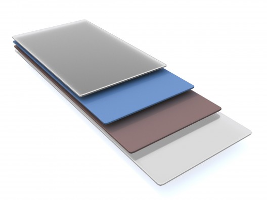
Researchers at the Vienna University of Technology have combined two semiconductor materials, each only three atomic layers thick. Adding one semiconducting layer of the photoactive crystal tungsten diselenide to a layer of molybdenum disulphide, and “creating a designer-material that may be used in future low-cost solar cells.”

Layered look of Vienna semiconductor sausage. Thomas Mueller and colleagues combined slices of tungsten diselenide and molybdenum disulphide to create transparent solar collector with a weight of one gram for over 3,300 square feet
Having worked with graphene, that two-dimensional, atom-thick material that promises much for structures, batteries and solar cells, Thomas Mueuller, assistant professor of photonics, and his team “acquired the necessary know-how to handle, analyze and improve ultra-thin layers by working with graphene.” The team applied their lessons learned with graphene to combining two ultra-thin semiconductor layers and are now studying their optoelectronic properties.
Mueller explains, ““Quite often, two-dimensional crystals have electronic properties that are completely different from those of thicker layers of the same material.” In their present study, the Tungsten diselenide, a semiconductor consisting of three atomic layers; one layer of tungsten sandwiched between two layers of selenium atoms. Mueller adds, “We had already been able to show that tungsten diselenide can be used to turn light into electric energy and vice versa.”
To get around the problem of inserting “countless tiny metal electrodes tightly spaced only a few micrometers apart,” the researchers came up with an “elegant” solution, combining the tungsten diselenide with molybdenum disulphide, which also consists of three atomic layers. The two three-layered slices can now form large-areas solar cells.
Vienna UT explains the interaction of the two layers: “When light shines on a photoactive material single electrons are removed from their original position. A positively charged hole remains, where the electron used to be. Both the electron and the hole can move freely in the material, but they only contribute to the electrical current when they are kept apart so that they cannot recombine.

(Left to right) Marco Furchi, Thomas Mueller, and Andreas Pospischil sort out how to combine multiple layers of semiconductors
“To prevent recombination of electrons and holes, metallic electrodes can be used, through which the charge is sucked away – or a second material is added. ‘The holes move inside the tungsten diselenide layer, the electrons, on the other hand, migrate into the molybednium disulphide’, says Thomas Mueller. Thus, recombination is suppressed.”
To tune the layers for proper alignment, Florian Libisch and Professor Joachim Burgdörfer provided computer simulations to calculate how the energy of the electrons changes in both materials and which voltage leads to an optimum yield of electrical power.
Mueller noted the challenge of stacking the two layers. “If there are any molecules between the two layers, so that there is no direct contact, the solar cell will not work.” In something like miniaturized vacuum bagging, researchers heated both layers in a vacuum and stacked them in ambient temperature, then reheated the layers to remove any water between the layers.
The resulting material allows incoming light to pass through it, and absorbs the rest, converting it into electricity. Transparent, the material could be used for window glass or for coatings on almost anything else, it would seem. Because it’s only a few atoms thick, 300 square meters (3,229 square feet, or about 32 sailplane wings) weigh a gram.
Researchers are now working on stacking more than two layers, which will reduce transparency but increase electrical power. How many layers will it take to make this a still lightweight but extremely powerful solar energy producer? We’ll anxiously await further developments from Vienna.
