
A good deal of what we see in life is counter-intuitive – things like pushing forward on the control stick when the airplane stalls and is headed downhill already. Plasmonic metamaterials as designed by University of Pennsylvania scientists have counter-intuitive properties, such as breaking light that strikes them into surface plasmon polaritons with shorter wavelengths than the original incident light.
This quantum-like reaction occurs when, “Light hitting a metamaterial is transformed into electromagnetic waves of a different variety—surface plasmon polaritons, which are shorter in wavelength than the incident light. This transformation leads to unusual and counterintuitive properties that might be harnessed for practical use. Moreover, new approaches that simplify the fabrication process of metamaterials are under development. This work also includes making new structures specifically designed to enable measurements of the materials’ novel properties. Furthermore, nanotechnology applications of these nanostructures are currently being researched, including microscopy beyond the diffraction limit.”
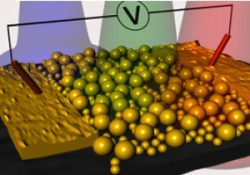
Plasmonic metamaterials rely on gold and other particles of carefully selected and varying sizes to conduct electricity efficiently
Scattering,rather than gathering light rays, seems counter-intuitive, but the scattering apparently allows the bouncing rays to achieve other wavelengths and increase the chance that the different sized materials will be able to capture energy from them. Various other solar cell researchers use different means to pull in a broader range of light’s wavelengths, but this approach promises to be simpler and much more efficient.
Dawn Bonnell, Penn’s vice provost for research and Trustee Professor of Materials Science and Engineering in the School of Engineering and Applied Science, explains, “We’re excited to have found a process that is much more efficient than conventional photoconduction. Using such an approach could make solar energy harvesting and optoelectronic devices much better.”
The study was published in the journal ACS Nano, focusing on plasmonic nanostructures – in this case materials fabricated from gold particles and light-sensitive molecules of porphyin, of precise sizes and arranged in specific patterns.
Samples showing varying sizes and arrangements of gold and other nanomaterials in Dawn Bonnell’s and associates’ research
“Plasmons, or a collective oscillation of electrons, can be excited in these systems by optical radiation and induce an electrical current that can move in a pattern determined by the size and layout of the gold particles, as well as the electrical properties of the surrounding environment.
Because these materials can enhance the scattering of light, they have the potential to be used to advantage in a range of technological applications, such as increasing absorption in solar cells,” according to the paper.
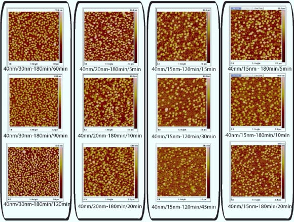
In a 2010 paper, Bonnell and her colleagues reported in ACS Nano that their arrays of gold nanoparticles, produced with a technique called ferroelectric nanolithography, could induce and project an electric current across molecules. They couldn’t prove the “hot electrons” produced by the excited plasmons caused this activity at the time, but their current research has demonstrated this actual reaction.
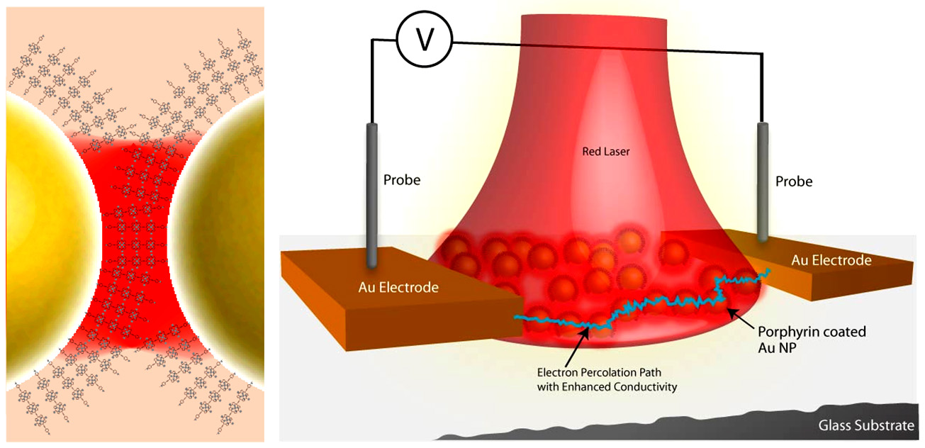
Diagram of 2010 experiment shows Dawn Bonnell’s early research into plasmonic behavior
The University notes Bonnell’s conjectures: “We hypothesized that, when plasmons are excited to a high energy state, we should be able to harvest the electrons out of the material. “If we could do that, we could use them for molecular electronics device applications, such as circuit components or solar energy extraction.”
Researchers, “Systematically varied the different components of the plasmonic nanostructure, changing the size of the gold nanoparticles, the size of the porphyin molecules and the spacing of those components. They designed specific structures that ruled out the other possibilities so that the only contribution to enhanced photocurrent could be from the hot electrons harvested from the plasmons.”
“’In our measurements, compared to conventional photoexcitation, we saw increases of three to 10 times in the efficiency of our process,’ Bonnell said. ‘And we didn’t even optimize the system. In principle you can envision huge increases in efficiency.’”
Bonnell sees various ways of customizing the materials. “You could imagine having a paint on your laptop that acted like a solar cell to power it using only sunlight. These materials could also improve communications devices, becoming part of efficient molecular circuits.”
Her work, with David Conklin, a doctoral student, involved a collaboration among additional Penn researchers, through the Nano/Bio Interface Center, as well as a partnership with the lab of Michael J. Therien of Duke University.
The Penn team included Bonnell, Conklin, Sanjini Nanayakkara and Xi Chen from Engineering’s Department of Materials Science and Engineering and Tae-Hong Park from the School of Arts and Sciences’ Department of Chemistry. Other coauthors included Marie F. Lagadec from ETH Zurich and Therien and Joshua T. Stecher of Duke.
The research was supported by the U.S. Department of Energy and the National Science Foundation.